
Lead Organisation: University of Cardiff
Project Lead: Peter Hargrave
Partners: University of Cambridge
The goal of this programme of work was to develop the concept of on‐chip superconducting filterbank spectrometers, coupled to transition‐edge superconducting (TES) sensors, and to demonstrate their key functionality. The major envisaged end‐user applications areas are to meteorology (temperature & humidity sounding), and climatology (ice‐cloud studies).
The primary novelty compared to other emerging solutions is that this is, to our knowledge, the first demonstration of a filterbank system based on TES technology. Filterbank spectrometers are under development for astronomy applications, but these are based on kinetic inductance detector (KID) technology. The issue with KID‐based technology solutions is that the photon energy required to break a Cooper pair in the superconducting film (and hence a detector response) limits the application to photon frequencies above around 100GHz. TES devices are not pair‐breaking detectors, but are very sensitive broad‐band power detectors (bolometers). The major advantage of using a TES based solution is that it can provide full access to the critically important atmospheric temperature sounding (O2) lines around 50‐60GHz. The key goal of this programme of work was to demonstrate performance in the 50‐60GHz region.
Initial work identified where improvements in temperature and humidity sounding could be made in comparison with existing technology solutions for NWP (numerical weather prediction), including the predicted impact of such improvements.
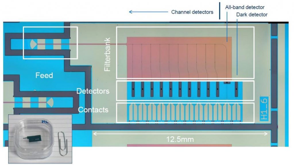
From these requirements, a series of on‐chip filterbank/TES devices with a range of spectral characteristics were designed and modelled. A total of eight filterbank chips were manufactured on a single wafer in the University of Cambridge Quantum Sensors Group’s clean rooms. The eight devices differ only in the design of the filterbank sections.
All of the films were deposited by either DC or RF sputtering, using deposition systems dedicated to superconducting electronics fabrication. These have been calibrated to give high quality, low stress, films with highly repeatable characteristics. Patterning of the layers was carried out by photolithography (minimum feature size = 0.25 μm) and a mixture of wet and dry etching and lift‐off processes. A total of twelve photolithography steps were performed.
All chips from the wafer are suitable for full RF measurements. Despite being the first fabrication run and the inclusion of several new processing steps and features, the total yield of detectors surviving processing was over 92%. Several chips have all detectors present. A second wafer was also taken through processing as a back‐up.
The devices were tested in a dedicated test facility built by Cardiff University. The chips were mounted into a bespoke packaging block. The packaging block was precision engineered in Cardiff, with extremely tight tolerances, particularly on the waveguide section. The filterbank was fed via a waveguide probe. This probe was placed in the machined waveguide, and coupled to a vector‐network analyser (VNA) system. The TES detectors were read‐out via cold electronics, utilising SQUID devices (Figure 3), coupled to warm electronics. The filterbank/detector block was mounted in the test facility in Cardiff, and tested at 300mK. The VNA signal was fed from outside the test cryostat via stainless steel and superconducting coaxial cables, certified for operation up to 70GHz, and coupled via a coax‐to‐waveguide transition.
The device tested had nine channels connected, limited by the available number of SQUIDS in the readout electronics. The channels connected covered the range 42.5 – 60GHz.
Spectral response measurements were made by frequency‐sweeping an RF signal from the VNA through the connected filterbank. The channels fall almost where expected, with approximately the correct Qvalue. The response to different RF power level frequency sweeps was also measured. This single detector shows the response from all other channels, in terms of the power at filterbank frequencies that is diverted into the individual filter channels. This response shows clearly that all channels on the manufactured filterbank chip are active, even showing the response from the non‐connected channels.
The team has demonstrated the first ever on‐chip filterbank based on TES devices. The performance of the test device is almost exactly in line with modelling predictions. Moreover, the device yield was 100%, with all filter channels active, and performing to expectations. There is a small, but consistent offset between the modelled and measured channel position and Q‐factor. This is due to small uncertainties in the material parameters used in the modelling. The results from this project will enable the team to constrain those material parameters for future device manufacture.